


Research
KrusinLab - Quantum transport and spin response of topological materials and devices
Topological insulators are a recently discovered unique class of quantum solids with immune-to-disorder spin-helical metallic surface states having Dirac band structure and ideally having insulating bulk. The robustness and spin polarization of the unusual topological surfaces is potentially transformative in the fields of spin-based nanoelectronics and fault-tolerant quantum computing.
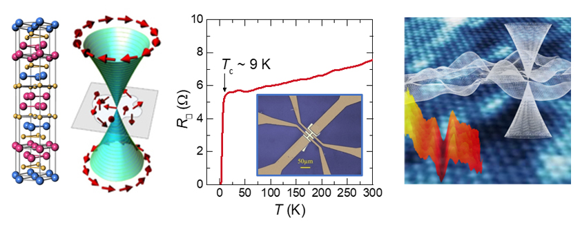
In Krusin group we were the first to uncover a singular and highly tunable response of Dirac spins (Nature Materials 13, 580 (2014)), an emergent high-temperature superconductivity of surface Dirac charge puddles (Nature Comm. 6, 8279 (2015)), both a remarkable quantum phenomena made visible through disorder. Bulk disorder, however, is presently the biggest challenge to accessing surface charge transport - the ubiquitous lattice imperfections donate charge carriers that intermix with surface Dirac particles and pull Fermi energy level into the bulk bands. To address this we have developed a new approach that uses high energy (2.5 MeV) electron beams to compensate charged bulk defects and bring the Fermi level back into the bulk gap (Nature Comm. 7, 10957 (2016)) . This enabled us to achieve a stable charge neutrality point using electron beams with long reach, thereby establishing a route to intrinsic quantum transport of the topological states unconstrained by the bulk size.
MerilesLab - New spin-based platforms for nanometer-resolution MRI and sensing
With applications ranging from high-resolution sensing to quantum information science, spin control at the nanoscale is emerging as an area of newfound importance. Work at the Meriles group focuses on (i) the development of new spin-based platforms for nanometer-resolution MRI and various nanoscale sensing protocols, (ii) quantum control of individual spin clusters for quantum information processing and spintronics, (iii) the generation of electron or nuclear spin hyper-polarization, and (iv) the investigation of new material platforms hosting promising paramagnetic centers and single photon emitters.
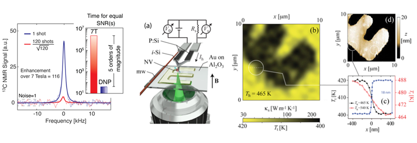
1. We use an optical-pumping protocol at room temperature to enhance the nuclear spin polarization of 13C spins in a diamond powder by more than one hundred times. This is an important step towards the use of diamond as a source for hyperpolarized fluids on-demand. A. Ajoy, K. Liu, R. Nazaryan, X. Lv, B. Safvati, G. Wang, D. Arnold, G. Li, A. Lin, P. Raghavan, E. Druga, D. Pagliero, J.A. Reimer, D. Suter, C.A. Meriles, A. Pines, submitted.
2. We combine use a diamond nanoparticle-hosted NV center as a probe to measure thermal conductivity of an arbitrary substrate. Our technique combines magnetic resonance with confocal and atomic force microscopy to attain a resolution of 10 nm under ambient conditions (Nature Comm. 6, 8954 (2015) ).
3. We are exploring alternative pathways to on-chip quantum information processing at room temperature using paramagnetic centers in diamond. The above image summarizes our most recent proposal based on the ionization and transport of charge carriers between separate spin clusters (Phys. Rev. X 6, 041035 (2016) ).
4. We use multi-color confocal microscopy to store information within diamond in three dimensions. Our approach exploits the variable response of NV centers in different charge states, which we can alter and readout an arbitrary number of times. The ultimate goal is to extend these techniques to the sub-diffraction limit by exploiting the NV spin degree of freedom (Science Adv. 2, e1600911 (2016)).
5. We use laser pulses of variable wavelength, intensity and duration to alter the charge state of paramagnetic centers in diamond and subsequently image the charge carrier redistribution. The image shows the concentration of negatively charged NVs upon illuminating a point at the interface between NV--rich and NV--depleted regions (Nature Comm. 7, 12660 (2016)).
6. The negatively-charged silicon-vacancy (SiV-) center is a defect of emerging importance for quantum information processing. The image shows our ability to reversibly control the charge state from negative to neutral (S. Dhomkar, P. Zangara, J. Henshaw, C.A. Meriles, submitted).
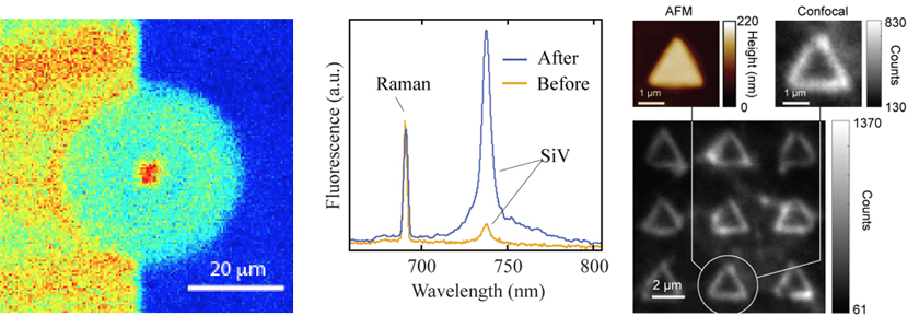
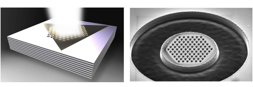
7. We are exploring (in collaboration with Vinod Menon) the properties of single-photon emitters in new material platforms. The image shows our ability to locally activate emitters in 20-nm-thin hexagonal boron nitride - a 2D material isomorphic to graphene - via strain, in turn, induced via a substrate patterned to host triangular pillars (N. Proscia, Z. Shotan, H. Jayakumar, P. Reddy, M. Dollar, A. Alkauskas, M.W. Doherty, C.A. Meriles, V.M. Menon, submitted. Available as arXiv:1712.01352.)
VinodLab - Exploring light matter interaction at the nano scale
Research in the Laboratory for Nano and Micro Photonics (LaNMP) can be best summarized as exploration of light-matter interaction at the nanosale. The main research focus areas are development of: photonic structures that confine light and artificially engineered optical materials such as metamaterials and hybrid excitonic materials that display optical properties that surpass naturally occurring materials. These focus areas are motivated by the quest to develop next generation computing technologies including those that exploit the quantum property of light, ultrasensitive sensors for chemical and biological detection, and high efficiency energy transfer systems.
Recent breakthroughs in the group have included the demonstration of optical control of microcavities with valley degree of freedom (Nature Photonics, 2017), new class of artificial photonic media: photonic hypercrystals for enhancing spontaneous emission (PNAS, 2017; Nano Letters, 2016), strong light-matter interaction between one-atom layer thick material and light (Nature Photonics, 2015), active hyperbolic metamaterials (Optica, 2015), organic-inorganic hybrid materials which use photons for coupling (Physical Review Letters, 2014), control of light-matter interaction by using an idea from the field of topology in mathematics (Science, 2012), direct visualization of transport of energy carrying particles in organic solar cells (Nature Comm., 2014) and a flexible laser technology (US Patent # 8610103, 2013).
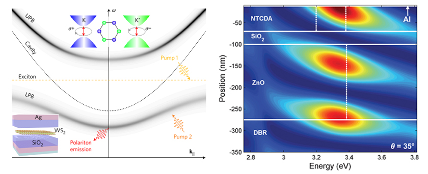
The realization of valley polaritons in 2D semiconductor microcavities presents the first step towards engineering valley-polaritonic devices. The left panels show the angle-resolved reflectivity, whereas the right panels show the angle-resolved PL obtained via Fourier space imaging. (a)-(f), The different detunings of the microcavities are Δ = –105 meV [(a), (b)]; Δ = – 60 meV [(c), (d)]; and Δ = +16meV [(e), (f)].

TamargoLab - MBE growth of electronic materials, topological insulators/heterostructures
The Tamargo group at City College conducts research on the molecular beam epitaxy (MBE) of novel electronic, photonic and spintronic materials. A broad range of materials and structures are grown using a three chamber molecular beam epitaxy growth system designed for the growth of As-based III-V semiconductors, wide bandgap II-VI semiconductors and 3D topological insulators, including Bi2Se3, Bi2Te3 and Sb2Te3. Several directions of research in quantum materials and nano-heterostructures are currently pursued. Materials characterization tools available on site include photoluminescence, High resolution X-ray diffraction, Hall Effect, Fourier Transform infrared spectroscopy and contactless electro-reflectance. Other techniques available through shared facilities include scanning and transmission electron microscopy and scanning probe microscopies
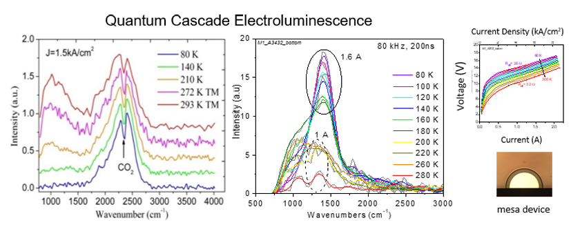
1. Growth of intersuband II-VI quantum cascade devices and hybrid II-VI/III-V heterostructures and devices. Intersubband (ISB) devices rely on transitions between quantum levels within one band (conduction or valence band) for their operation rather than more typical band-to-band transitions. They provide unique characteristics, such as ultra-fast response, reduced temperature sensitivity, etc., that make them attractive for advanced photonic applications. (Appl. Phys. Lett. 107, 141105 (2015); Phys. Status Solidi b 253, 1494 (2016) ).
2. These II-VI materials are grown lattice-matched to InP, which is also the substrate employed in the III-V ISB devices. To further expand the range of properties that can be achieved with these materials systems, our groups have recently demonstrated an all-lattice matched ultra-broad QC detector by combining two devices in a single hybrid II-VI/III-V structure. (Y. Kaya and C. F. Gmachl, II-VI and II-VI/III-V hybrid intersubband devices, (Invited) ITQW 2017, Singapore, September 10-16, 2017.).
3. Growth of submonolayer type-II quantum dots and quantum wells for photonic device applications and photovoltaics. Type-II quantum dots (QDs) and quantum wells (QW) offer unique properties over more well-studied type-I nano heterostructures. Among these, the separation of charge carriers is of interest for applications such as photovoltaincs. Our group, in collaboration with the Kuskovsky group at Queens College, has investigated the growth and properties a range of type-II quantum structures made from the II-VI semiconductor family of materials. Novel physical phenomena, such as ultra-high p-type doping of ZnSe, the Aharonov-Bohm (A-B) effect, and spin lifetime enhancements have recently been reported in these materials. One possible application of these nanostructures is the demonstration of a novel high efficiency photovoltaic device known as an intermediate band solar cell (IBSC). Our results indicate that our type-II QD materials have the most promise of any materials being explored for the demonstration of this unique device. (J. Appl. Phys. 116, 164308 (2014); Appl. Phys. Lett. 107, 251905 (2015); J. Applied Physics 121, 115702 (2017); Sol. Energ. Mat. Sol. C 117, 604 (2013) ).

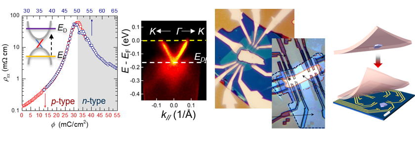
4. Growth of II-VI/TI heterostructures. Bi2Se3, Bi2Te3, Sb2Te3 and related ternary materials are part of a family of materials known as topological insulators (TIs). These materials are bulk semiconductors that have metallic surface states, which exhibit unique time reversal symmetry and spin-momentum locking. These properties make them highly promising for quantum computing and spintronic applications. Furthermore, novel physical phenomena, such as the existence of Marjorana fermions are theoretically predicted in these materials. Our group, in collaboration with Krusin group, is exploring the growth of these materials by MBE. In particular, we recently demonstrated for the first time the growth of superlattices of TIs and trivial semiconductors such as ZnSe and ZnCdSe with high structural quality. These SLs exhibit preserved topological surface states (Nano Letters 15, 6365 (2015) ). The potential for these heterostructures as a means of band engineering of the unique physical properties of the TI materials is being explored, with emphasis on enhancing the thermoelectric properties by Dirac bandgap engineering.
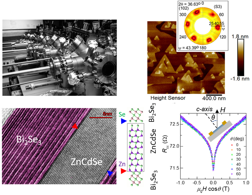
Various efforts are being pursued to optimize the nucleation and growth on various substrates, growth of multilayers and superlattices of TIs, such as Bi2Se3/Bi2Te3 and Bi2Se3 /Sb2Te3, growth of ternary and quaternary alloys of the general structure (Bi,Sb)2(Te,Se)3. Investigations of these materials from a structural perspective, using AFM, high resolution XRD, and TEM as well as their transport physics by low temperature Hall and magnetotransport measurements is being pursued. (Phys. Stat. Sol. b 79, 1700275 (2017)). Presently we are working on thin topological films and superlattices for photonic applications (collaboration with Menon and Krusin groups) of interest to HCQM.
KhanikaevLab - Optical excitations in plasmonic nanostructures and metamaterials
Khanikaev group focuses on experimental research and theoretical studies of photonic nanostructures and metamaterials aiming to develop novel optical systems and devices with previously unattainable properties and useful functionalities. The research includes an interdisciplinary studies at the edge of optics and such disciplines as biology and condensed matter physics. One of the major research directions is engineering topological order and nonreciprocity in photonic nanostructures with magneto-optical and bianisotropic responses. The bio-oriented research program of the group is aiming to facilitate in-depth characterization of bio-molecules with the use infrared spectroscopy of plasmonic nanostructures and metamaterials.
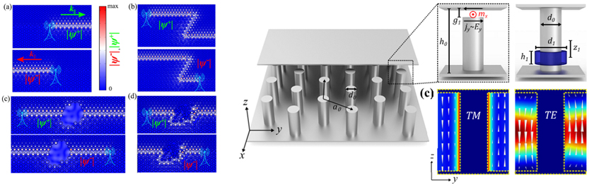
Guiding Electromagnetic Waves around Sharp Corners: Topologically Protected Photonic Transport in Metawaveguides.
Bianisotropic metawaveguide (BMW) as a photonic topological insulator. Schematic of the BMW. Part of the top metal plate is removed to reveal the“bed-of-nails”structure below. The enlarged regions on the right illustrate the origin of the bianisotropic response. Right inset: an equivalent way to produce bianisotropy by adding an asymmetrically placed metallic volume (washer) around the rod. (Physical Review Letters 114, 127401 (2015) ).
Topologically protected elastic waves in phononic metamaterials (Nature Comm. 6, 8682 (2015) )
Current focus of the group is photonic topological insulators. A remarkable and useful property of solid-state topoogical materials is that they support unidirectional spin-polarized propagation at their surfaces. Using suitably designed electromagnetic media (metamaterials) We have theoretically demonstrated a photonic analogue of a topological insulator. We showed that metacrystals—superlattices of metamaterials with judiciously designed properties—provide a platform for designing topologically non-trivial photonic states, similar to those that have been identified for condensed-matter topological insulators. The interfaces of the metacrystals support helical edge states that exhibit spin-polarized one-way propagation of photons, robust against disorder. Our results demonstrate the possibility of attaining one-way photon transport without application of external magnetic fields or breaking of time-reversal symmetry. Such spin-polarized one-way transport enables exotic spin-cloaked photon sources that do not obscure each other.
Topologically protected elastic waves in phononic metamaterials (Nature Comm. 6, 8682 (2015) )
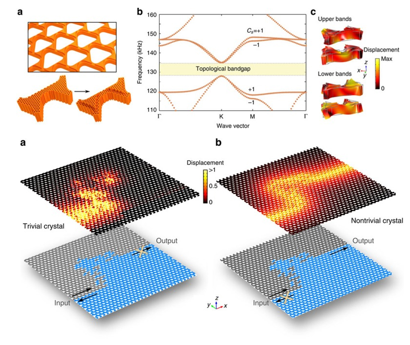
Spin-orbit coupling and bandgap opening by breaking mirror symmetry σz. (a) Perspective view of the modified phononic crystal (upper panel) with broken z-mirror symmetry: the top rim of each air hole is enlarged into a counterbore (lower panel) with 14% increase in size and a 20% depth of the overall thickness. The overall thickness is increased to 2.94 mm to restore the spin degeneracy between the modes at the K-point. (b) Phononic band structure showing a complete bandgap (5.4% relative bandwidth) induced by the symmetry breaking. Phase and group velocities at the band edge remain matched near the K-point. Spin Chern number CS, calculated using first-principle finite-element method simulations, is shown for each band. (c) Displacement fields of a unit cell at the Dirac point (K), illustrating the hybridization between the S and A modes. Colors indicate the absolute value of the displacement..
Topologically trivial and nontrivial edge modes facing a one-dimensional random potential. (a) Trivial crystal is designed with the triangular holes rotated by 12.5° clockwise (grey region) and anticlockwise (blue region). To create the bandgap in the same spectral range as in the nontrivial case, the structure is scaled up by factor of 1.07% in all geometrical parameters. In this structure with mirror symmetry, the symmetric mode is excited. (b) The nontrivial crystal. The excitation frequency in both panels is 130.5 kHz.
Spin-polarized phononic helical edge state from external loads. (a) External force fields on the truncated boundary of a topological crystal exposed to vacuum, which supports only the spin-up phonons travelling in the anticlockwise manner. The force amplitude is shown in pseudocolor, and the inset illustrates the force directions (blue for outward directions and red for inward directions). (b) Displacement fields of the resultant spin-up mode excited by a source located at the lower left corner of the crystal. Impedance-matched absorbers are used on the upper-left corner to absorb the output wave.
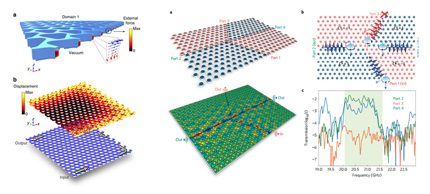
Robust reconfigurable electromagnetic pathways within a photonic topological insulator The discovery of topological photonic states has revolutionized our understanding of electromagnetic propagation and scattering. Endowed with topological robustness, photonic edge modes are not reflected from structural imperfections and disordered regions. Here we demonstrate robust propagation along reconfigurable pathways defined by synthetic gauge fields within a topological photonic metacrystal. The flow of microwave radiation in helical edge modes following arbitrary contours of the synthetic gauge field between bianisotropic metacrystal domains is unimpeded. This is demonstrated in measurements of the spectrum of transmission and time delay along the topological domain walls. These results provide a framework for freely steering electromagnetic radiation within photonic structures (Nature Materials 15, 542 (2016) ) .
Experimental demonstration of spin-locked wave-division of an edge mode at a four-port topological junction. a, Top: four-port configuration formed by the four topological domains with collars shifted up (red) and down (blue). Bottom: The results of numerical modelling of the spin-locked wave-division. b, Spin locking ensures that the spin-down edge mode excited at Port 1 can escape only along the two (out of three) domain walls for which the direction of propagation for the edge mode agrees with the spin, leading to coupling only to Ports 2 and 4 with the compete suppression of transmission through Port 3. c, Experimental transmission spectra at output Ports 2, 3 and 4 due to edge modes propagating along the respective domain walls indicated by black dashed lines in a. As before, the green shaded regions indicate the topological bandgap (Nature Materials 2016) ).
Ganeshan Theory Group - Strongly correlated topological matter, many-body localization, and quantum thermalization
Phases of matter manifesting robust quantum effects at a macroscopic scale have been at the frontier of our understanding of a multitude of emergent phenomena. Among several phenomena manifesting macroscopic quantum effects, topological quantization and Anderson localization have been at the forefront of both theoretical and experimental research due to their importance to fundamental physics and to the wealth of potential technological applications they enable. Ganeshan group research program in the past two years has focused on strongly correlated topological phases of matter, many-body localization, and quantum thermalization. Candidate systems realizing these theoretical pursuits are strongly correlated quantum materials like GaAs heterostructures, Graphene, and photonic materials (Phys. Rev. Lett. 2017; Nature Photonics 2016; Phys. Rev. Lett. 2015; Phys. Rev. B 2015)
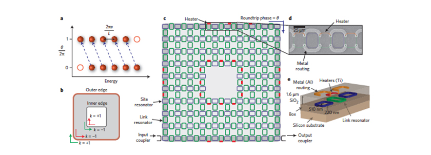
Schematic of the set-up used to measure the winding number. (a) Spectral flow of edge states with coupled gauge flux θ for q = 1 and k = 1. When θ = 2π edge states move by one position. (b),(c) Square annulus of coupled ring resonators that implements the integer quantum Hall effect, with an outer edge of 10 sites and an inner edge of 4 sites. The uniform synthetic magnetic field for photons is introduced by positioning the link rings. The system exhibits two pairs of CW and ACW propagating edge states, one each on the outer and inner edges. The tunable gauge field coupled only to the edge states is introduced by fabricating heaters on link resonators situated at the lattice edges. The total flux θ introduced by the heaters is the sum of the individual phases incurred in the link resonator arms. (d) SEM image showing the heaters fabricated on top of the link resonators (green). (e) Schematic of the waveguide cross-section showing the ring resonators, the metal heaters, and the metal routing layer.
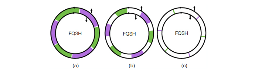
(a) A fractional quantum spin Hall edge in proximity to alternating ferromagnetic and superconducting strips (b-c). By shrinking the size of the ferromagnetic and superconducting strips while at the same time increasing the strength of the proximity coupling, we can continuously deform the system into a fractional quantum spin Hall edge with magnetic and superconducting impurities.
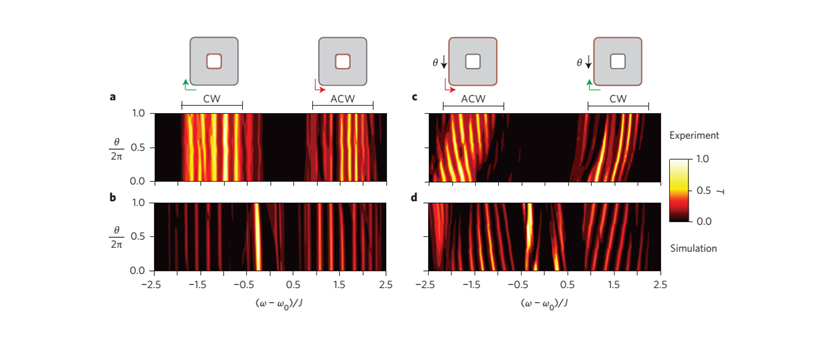
Local nature of coupled gauge flux and spectral flow for spin-flip excitation. Measured (a) and simulated (b) transmission spectra (linear scale, normalized to unity) as a function of θ when only the inner edge is heated. The transmission resonances of the edge states associated with the outer edge do not change. Measured (c) and simulated (d) transmission spectra for spin-down excitation. The CW and ACW circulating states have now exchanged positions and move in opposite directions, giving k = 1.2 (2) for the CW edge band and k = −1.2 (2) for the ACW band. The transmission spectra shown in (a) and (c) are from two different devices.
Measurement of topological invariants in a 2D photonic system, Sunil Mittal, Sriram Ganeshan, Jingyun Fan, Abolhassan Vaezi, Mohammad Hafezi, Nature Photonics 10, 180183 (2016) (featured on the cover of Nature Photonics).
Ghaemi Theory Group - Topological phases of matter, Strongly correlated materials
During the last few decades, many new phases of matter which cannot be classified using Landau paradigm were discovered. These phases are identified by their topological characteristics and have potential applications for the development of new technologies such as quantum computers and spintronic devices. Ghaemi group is interested in the study of the interaction of topological phases with light, as well as their interplay with superconductivity and magnetism. Ghaemi also works on strongly correlated quantum materials, such as pnictide superconductors and Kondo lattice materials.
Some of our recent results are the realization of light-induced fractional Hall phases in graphene (Phys. Rev. Lett. 2017), explanation of the enhancement of electronic quantum coherence through strong interaction with light (Nature Photonics 2017), effect of impurities on Josephson junctions built on topological insulators (Phys. Rev. Lett. 2016) and studies of magnetic oscillations in strongly-interacting topological Kondo insulators (Phys. Rev. Lett. 2016).
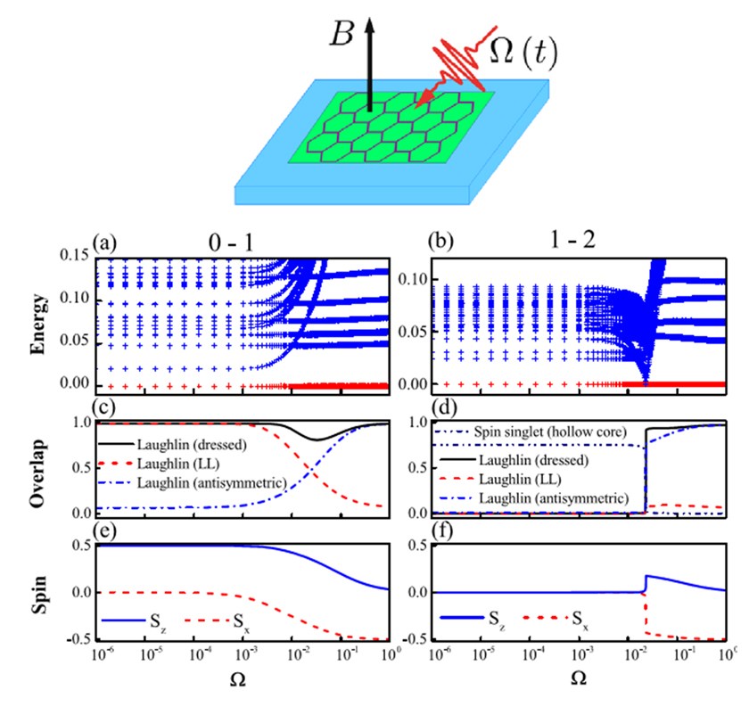
Light induced quantum phase transition between fractional Hall phases in graphene. The transition is tuned by the intensity of the light. (a),(b) Energy levels (above the ground state in units of e2 = εlB) vs Rabi frequency Ω, for coupling LL0-1 (a) and LL1-2 (b). (c),(d) Ground state overlaps with trial wave functions (particle-hole conjugate 1/3 Laughlin state and a singlet phase obtained from the hollow-core model). Trial states are constructed in three different bases: (i) LL basis. All the electrons reside in the lower LL. (ii) Dressed basis. All electrons reside in lower eigenstates . (iii) Antisymmetric basis. All electrons reside in the singlet state. (e),(f) Spin polarization Sα of the ground state vs Ω for LL0-1(e) and LL1-2 (f). Data in all panels (a)–(f) were obtained for eight electrons on the torus, and δ = 0.02.